

0755-23504156
Hotline
Hotline

 Your location:Home > Products
> Route board proofing
Your location:Home > Products
> Route board proofing
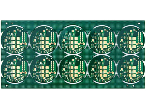
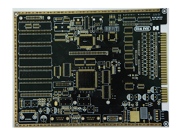
PCB proofing: 8L
Plate thickness: 2.0mm
Outer copper thickness: 3oz
Inner copper thickness: 2oz
Minimum hole diameter: 0.25mm
Minimum line width/line spacing: 5mil
Surface treatment: gold deposit
Product use: server power panel
Process difficulty: 3oz copper thickness 3rd order blind buried hole
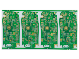
PCB proofing As the carrier of electronic components, the size and performance of the circuit board are determined by the number of layers of the multilayer board and the precision design degree of the circuit. This industrial robot adopts an 8-layer board design, with 3 mi l/3 mi l line width and line matching. At the same time, it encapsulates 10 groups of ICs and 12 groups of BGAs, which can be called a high-end product of high-precision printed circuit boards.
Main Process Characteristics of PCB Proofing Embedded Blind Orifice
1. Design of buried blind hole;
2. 3mil line width and line spacing;
3. BGA spherical design shall be uniform in size;
4. IC green oil bridge 4mil/4mil.
 Contact: Mr. Zheng
 Mobile phone: 13544145687
 Tel.: 0755-23504156
 Email: gypcb68@163.com
 Website: www.gydcpcb.com
 Address of Shenzhen Marketing Department: B212, Yinong Building, No. 4, Haoye Road, Qiaotou Community, Fuhai Street, Bao'an District, ShenzhenAddress of Chengdu Marketing Department: 14/F, Building B, Zijingnian, No. 5, Chuangye Road, High tech Zone, Chengdu, SichuanFactory address: Building 4, Wansha Industrial Park, Gonghe Village, Shajing Street, Bao'an District, Shenzhen
 Website