

0755-23504156
Hotline
Hotline

 Your location:Home > Products
> Security PCB
Your location:Home > Products
> Security PCB
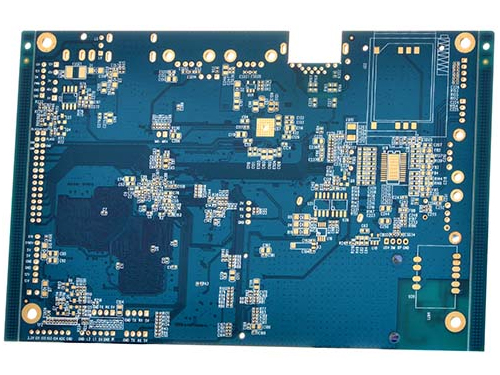
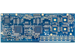
4-layer gold deposit security pcb layer number: 4 L
Plate thickness: 1.6mm
Outer copper thickness: 1 OZ
Inner copper thickness: 1 OZ
Minimum hole diameter: 0.3mm
Minimum line width/line spacing: 4mil
Surface treatment: gold deposit
Product application: video display
Process difficulties:/
Advantages of 4-layer gold deposit security pcb products:
1. Top technical team with rich production experience in precision multilayer circuit board
All the staff have professional and technical talents with many years of PCB experience and superb technology
2. Leading process capability to meet the demand for precision multilayer PCB manufacturing
Maximum thickness diameter ratio 10:1 Maximum copper thickness 6OZ Maximum working plate size 2000x610mm
The thinnest 4-ply plate is 0.33mm, and the smallest mechanical hole/pad is 0.2/0.40mm
Drilling accuracy/-0.05mmPTH hole diameter tolerance/-0.05mm
Minimum line width/line spacing 0.075/0.075mm
3. Advanced automatic production equipment and precision inspection equipment are specially equipped with a full set of surface treatment production lines for precision multilayer boards
Few in the industry are equipped with a full set of surface treatment equipment (gold, silver, tin, OSP, tin spraying, gold plating and thick gold plating, tin plating and silver plating) to reduce the risk of outsourcing production for you
4. Strict quality control system ensures 100% qualified rate of delivery quality
Strictly implement the quality PDCA process, continuously improve the product performance, and strictly control in accordance with IPC standards
 Contact: Mr. Zheng
 Mobile phone: 13544145687
 Tel.: 0755-23504156
 Email: gypcb68@163.com
 Website: www.gydcpcb.com
 Address of Shenzhen Marketing Department: B212, Yinong Building, No. 4, Haoye Road, Qiaotou Community, Fuhai Street, Bao'an District, ShenzhenAddress of Chengdu Marketing Department: 14/F, Building B, Zijingnian, No. 5, Chuangye Road, High tech Zone, Chengdu, SichuanFactory address: Building 4, Wansha Industrial Park, Gonghe Village, Shajing Street, Bao'an District, Shenzhen
 Website