

0755-23504156
Hotline
Hotline
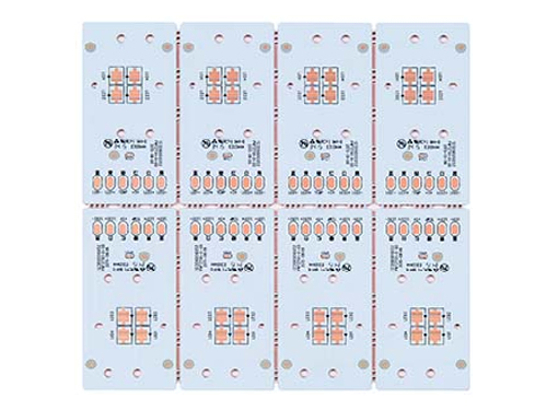
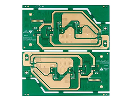
Number of layers: 1L
Plate thickness: 1.6mm
Outer copper thickness: 1OZ
Inner copper thickness:/
Minimum hole diameter: 1.70mm
Minimum line width/line spacing: 10mil
Surface treatment: osp
Product application: automobile power panel
Process difficulty: thermoelectric separation
Manufacturing characteristics of automobile PCB:
High frequency substrate
The vehicle anti-collision/predictive braking safety system plays the role of military radar equipment. Since the automobile PCB is responsible for transmitting microwave high-frequency signals, it is necessary to apply the substrate with low dielectric loss and common substrate materials together as PTFE. Unlike FR4 material, PTFE or similar high-frequency substrate material requires special drilling speed and feed speed during drilling.
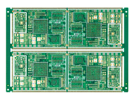
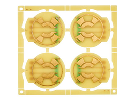
Thick copper PCB
Automobile electronic products bring more heat energy due to high density and high power. Hybrid power and motors often need more advanced power transmission systems and more electronic functions, which leads to more requirements for heat dissipation and large current.
It is relatively easy to manufacture thick copper double-layer PCB, while it is much more difficult to manufacture thick copper multilayer PCB. The key lies in thick copper image etching and thickness void filling.
The internal path of thick copper multilayer PCB is thick copper, so the pattern transfer photo induced dry film is also relatively thick, requiring great etching resistance. The etching time of thick copper pattern is long, and the etching equipment and technical conditions are in the best state to ensure the complete wiring of thick copper. When the manufacturing of external thick copper wiring is involved, the combination between copper foil with relatively thick lamination and pattern thick copper layer can be carried out first, and then the film gap etching can be carried out. The anti plating dry film of pattern coating is also relatively thick.
The surface difference between the inner conductor of thick copper multilayer PCB and the insulating substrate material and the ordinary multilayer board lamination is large, and the resin is not completely filled and the cavity is generated. To solve this problem, thin prepregs with high resin content should be coated as much as possible. The copper thickness of internal wiring on some multilayer PCBs is uneven, and different prepregs can be used in areas with large or small differences in copper thickness.
 Contact: Mr. Zheng
 Mobile phone: 13544145687
 Tel.: 0755-23504156
 Email: gypcb68@163.com
 Website: www.gydcpcb.com
 Address of Shenzhen Marketing Department: B212, Yinong Building, No. 4, Haoye Road, Qiaotou Community, Fuhai Street, Bao'an District, ShenzhenAddress of Chengdu Marketing Department: 14/F, Building B, Zijingnian, No. 5, Chuangye Road, High tech Zone, Chengdu, SichuanFactory address: Building 4, Wansha Industrial Park, Gonghe Village, Shajing Street, Bao'an District, Shenzhen
 Your location:
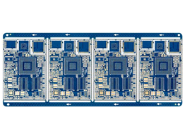
 Website