

0755-23504156
Hotline
Hotline
 Your location:Home > Products
> Route board proofing
Your location:Home > Products
> Route board proofing
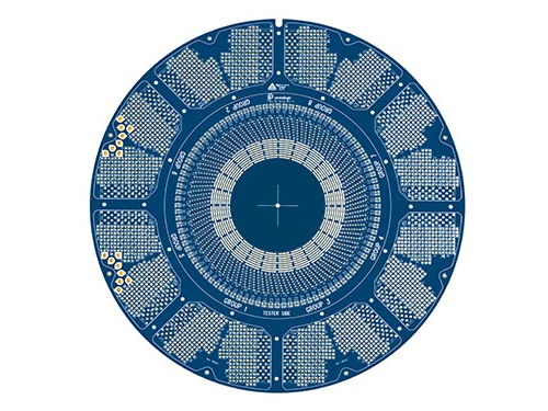
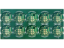
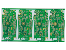
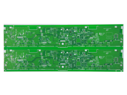
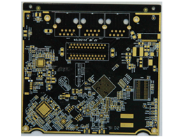
Number of PCB proofing layers: 26L
Plate thickness: 6.6mm
Outer copper thickness: 2 OZ
Inner copper thickness: 2 OZ
Minimum hole diameter 0.8mm
Minimum line width/line spacing: 3mil
Surface treatment: gold deposit
Product application: IC testing instrument
Process difficulty: high multilayer board
 Contact: Mr. Zheng
 Mobile phone: 13544145687
 Tel.: 0755-23504156
 Email: gypcb68@163.com
 Website: www.gydcpcb.com
 Address of Shenzhen Marketing Department: B212, Yinong Building, No. 4, Haoye Road, Qiaotou Community, Fuhai Street, Bao'an District, ShenzhenAddress of Chengdu Marketing Department: 14/F, Building B, Zijingnian, No. 5, Chuangye Road, High tech Zone, Chengdu, SichuanFactory address: Building 4, Wansha Industrial Park, Gonghe Village, Shajing Street, Bao'an District, Shenzhen
 Website