

0755-23504156
Hotline
Hotline
 Your location:Home > Products
> Communication PCB
Your location:Home > Products
> Communication PCB
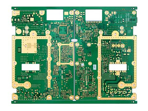
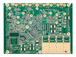
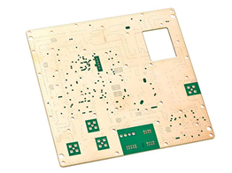
Communication RF pcb layer: 8L
Plate thickness: 1.6mm
Outer copper thickness: 1 OZ
Inner copper thickness: 1 OZ
Minimum hole diameter: 0.3mm
Minimum line width/line spacing: 5mil
Surface treatment: gold deposit
Product application: near-field communication
Process difficulty: mixed pressure structure
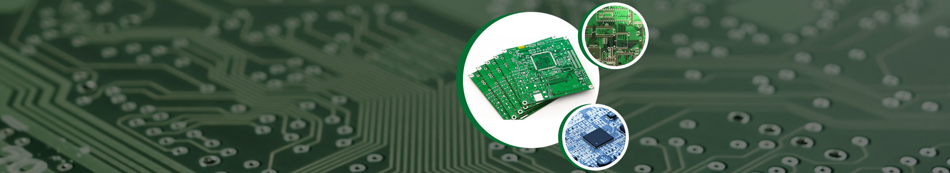
PCB is known as the "mother of electronic system products". As the basic material of electronic products, it has a broad demand market. Its downstream application fields cover communication, computer, consumer electronics, industrial control medicine, automotive electronics, aerospace, etc., of which communication and computer are the largest application plates of PCB at present, accounting for more than 25%.
PCB industrial chain
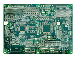
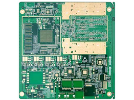
In the field of communication, PCB is widely used in wireless networks, transmission networks, data communications, fixed network broadband, and related PCB products involve backplanes, high-speed multilayer boards, high-frequency microwave boards, multi-functional metal substrates, etc.
 Contact: Mr. Zheng
 Mobile phone: 13544145687
 Tel.: 0755-23504156
 Email: gypcb68@163.com
 Website: www.gydcpcb.com
 Address of Shenzhen Marketing Department: B212, Yinong Building, No. 4, Haoye Road, Qiaotou Community, Fuhai Street, Bao'an District, ShenzhenAddress of Chengdu Marketing Department: 14/F, Building B, Zijingnian, No. 5, Chuangye Road, High tech Zone, Chengdu, SichuanFactory address: Building 4, Wansha Industrial Park, Gonghe Village, Shajing Street, Bao'an District, Shenzhen
 Website