

0755-23504156
Hotline
Hotline

 Your location:Home > Products
> Communication PCB
Your location:Home > Products
> Communication PCB
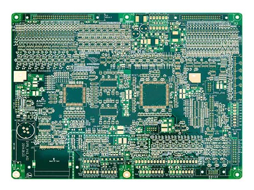
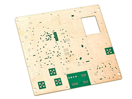
Number of communication pcb layers: 16L
Plate thickness: 4.0mm
Outer copper thickness: 1 OZ
Inner copper thickness: 1 OZ
Minimum hole diameter 0.50mm
Minimum line width/line spacing: 6mil
Surface treatment: gold deposit
Product application: control motherboard
Process difficulties: 22 groups of impedance
It is understood that the global communication PCB market will reach 14.799 billion US dollars in 2016, accounting for 27.3% of the total output of PCB. Among them, the proportions of single-sided, double-sided, 4-layered, 6-layered, 8-16-layered and over 18 years old were 11.98%, 17.62%, 12.49%, 35.18% and 7.26% respectively, with the total proportion reaching 84.5%. In 2014, due to the construction of 4G base stations, the output value of global communication printed circuit boards increased by 5.18% year on year, reaching the highest level in four years. 5G will be commercialized in 2019. Thanks to 5G, the future communication printed circuit board is expected to usher in a new round of rapid growth.
According to insiders, among 5G wireless base stations, operator networks, transmission networks and core network hardware facilities, PCB hardware applications will increase significantly. At the same time, 5G terminal devices, such as mobile phones and smart watches, should also be updated simultaneously with communication technology, which requires much more circuit boards than infrastructure.
 Contact: Mr. Zheng
 Mobile phone: 13544145687
 Tel.: 0755-23504156
 Email: gypcb68@163.com
 Website: www.gydcpcb.com
 Address of Shenzhen Marketing Department: B212, Yinong Building, No. 4, Haoye Road, Qiaotou Community, Fuhai Street, Bao'an District, ShenzhenAddress of Chengdu Marketing Department: 14/F, Building B, Zijingnian, No. 5, Chuangye Road, High tech Zone, Chengdu, SichuanFactory address: Building 4, Wansha Industrial Park, Gonghe Village, Shajing Street, Bao'an District, Shenzhen
 Website